This course provides an overview of the Semiconductor Technology manufacturing process. We divide this course into three sections: processing, packaging and testing. The processing section covers wafer fab processing techniques at a high level. These are the basic tools and techniques used to grow, etch, deposit, and pattern the thin films on a semiconductor or integrated circuit chip. For more detailed information on wafer fab processing techniques, please visit the Processing and Process Integration Classrooms located nearby in this system. The packaging section covers at a high level the basic techniques to package a semiconductor component into a form that can be used in an electronic system. These techniques including wire bonding, die attach, solder ball attach, molding, and so on. We also discuss the packaging design process and the various types of packages. For more detailed information on packaging techniques, please visit the Packaging Design and Packaging Technology Classrooms located nearby in this system. The testing section covers general information on how to test components. It includes an overview of the testing process and materials on various test techniques and design techniques like Scan-Based Testing. For more detailed information on testing techniques, please visit the Test Classroom located nearby in this system.

 This course provides an overview of the Semiconductor Technology
manufacturing process. We divide this course into three sections:
processing, packaging and testing. The processing section covers wafer
fab processing techniques at a high level. These are the basic tools and
techniques used to grow, etch, deposit, and pattern the thin films on a
semiconductor or integrated circuit chip. For more detailed information
on wafer fab processing techniques, please visit the Processing and
Process Integration Classrooms located nearby in this system. The
packaging section covers at a high level the basic techniques to package
a semiconductor component into a form that can be used in an electronic
system. These techniques including wire bonding, die attach, solder
ball attach, molding, and so on. We also discuss the packaging design
process and the various types of packages. For more detailed information
on packaging techniques, please visit the Packaging Design and
Packaging Technology Classrooms located nearby in this system. The
testing section covers general information on how to test components. It
includes an overview of the testing process and materials on various
test techniques and design techniques like Scan-Based Testing. For more
detailed information on testing techniques, please visit the Test
Classroom located nearby in this system.
This course provides an overview of the Semiconductor Technology
manufacturing process. We divide this course into three sections:
processing, packaging and testing. The processing section covers wafer
fab processing techniques at a high level. These are the basic tools and
techniques used to grow, etch, deposit, and pattern the thin films on a
semiconductor or integrated circuit chip. For more detailed information
on wafer fab processing techniques, please visit the Processing and
Process Integration Classrooms located nearby in this system. The
packaging section covers at a high level the basic techniques to package
a semiconductor component into a form that can be used in an electronic
system. These techniques including wire bonding, die attach, solder
ball attach, molding, and so on. We also discuss the packaging design
process and the various types of packages. For more detailed information
on packaging techniques, please visit the Packaging Design and
Packaging Technology Classrooms located nearby in this system. The
testing section covers general information on how to test components. It
includes an overview of the testing process and materials on various
test techniques and design techniques like Scan-Based Testing. For more
detailed information on testing techniques, please visit the Test
Classroom located nearby in this system.

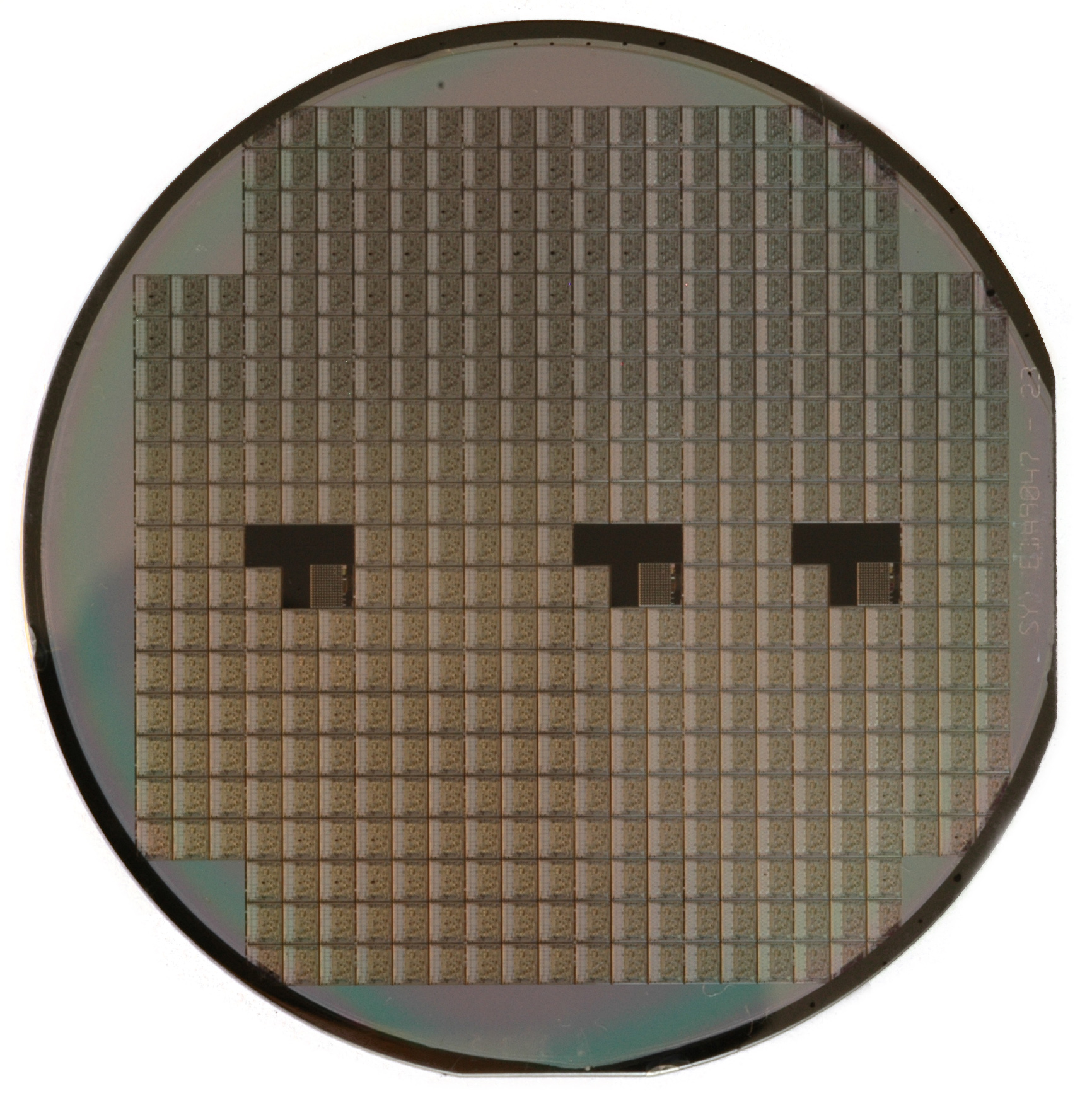
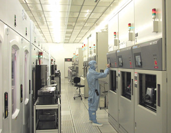 Fabrication of semiconductors and integrated circuits (ICs) is arguably one of the most advanced manufacturing processes ever developed. A state-of-the-art IC requires a ultra clean environment, ultra pure chemicals and gases, highly sophisticated fabrication tools, and a team with extensive knowledge of chemical engineering, semiconductor physics, modeling, and logistics management. The materials in this section cover the main disciplines or steps used in semiconductor fabrication. They include:
Growth and preparation of the starting material (Si, GaAs, or other semiconductor materials)
Diffusion
Oxidation
Cleaning
Ion Implantation
Lithography
Chemical Vapor Deposition
Physical Vapor Deposition
Chemical Mechanical Planarization
Please click on the topics to the left to begin learning about this fascinating process.
Fabrication of semiconductors and integrated circuits (ICs) is arguably one of the most advanced manufacturing processes ever developed. A state-of-the-art IC requires a ultra clean environment, ultra pure chemicals and gases, highly sophisticated fabrication tools, and a team with extensive knowledge of chemical engineering, semiconductor physics, modeling, and logistics management. The materials in this section cover the main disciplines or steps used in semiconductor fabrication. They include:
Growth and preparation of the starting material (Si, GaAs, or other semiconductor materials)
Diffusion
Oxidation
Cleaning
Ion Implantation
Lithography
Chemical Vapor Deposition
Physical Vapor Deposition
Chemical Mechanical Planarization
Please click on the topics to the left to begin learning about this fascinating process.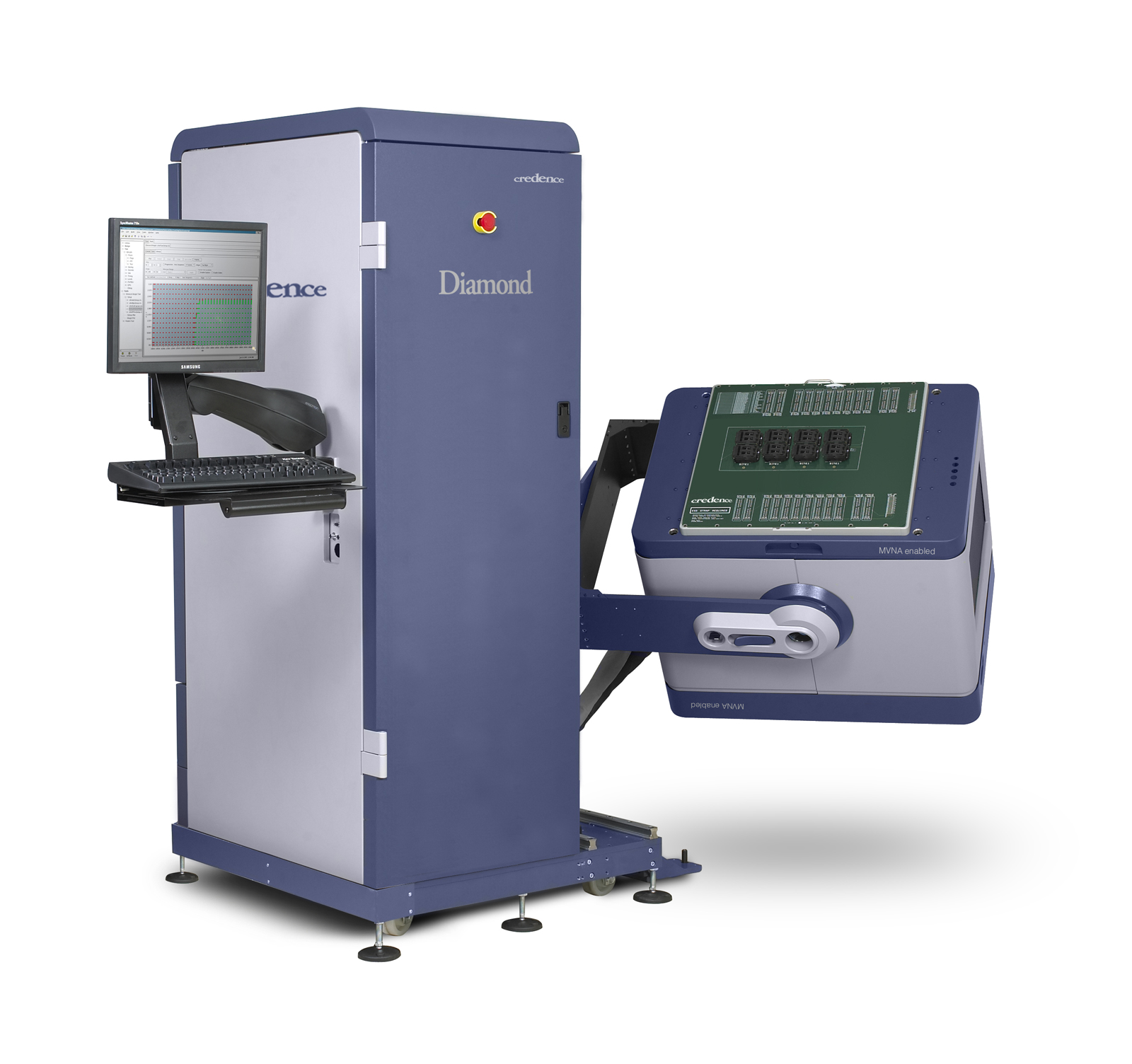

This section covers semiconductor and integrated circuit test. Test is a critical aspect of the design and manufacturing process. Test allows one to determine if the device is working correctly, and it can also give insight into potential failure mechanisms and manufacturing issues. In this section we cover: defect modeling, design for test, digital testing, analog testing, parametric testing, and test hardware.
Please click on the topics to the left to begin learning about this fascinating process.
