
If you wish to take a course to receive a certificate, you must take the course under "Online Courses". Do NOT take the course here under "Materials By Topic" as you would not receive a certificate for completing the materials here. The "Materials By Topic" content is intended just for reference purposes.
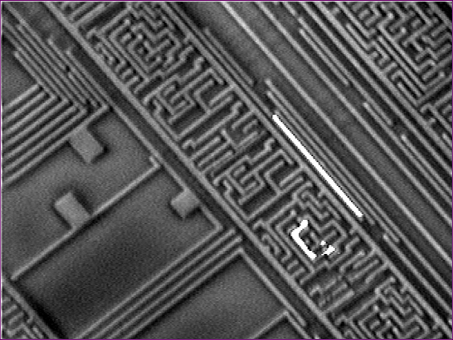
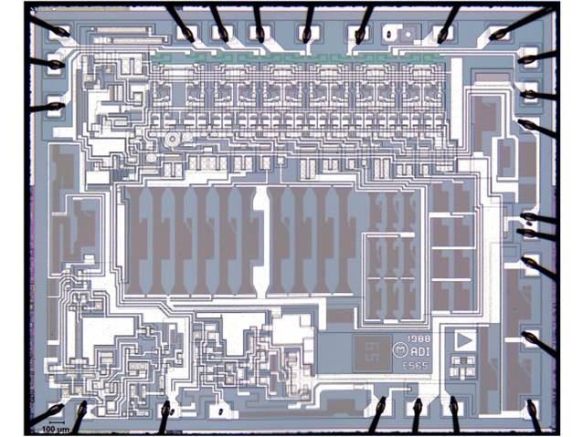
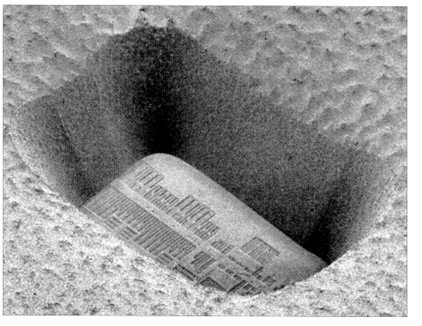
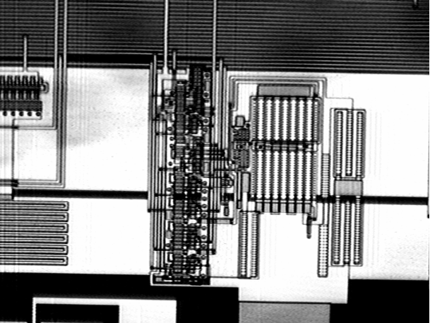
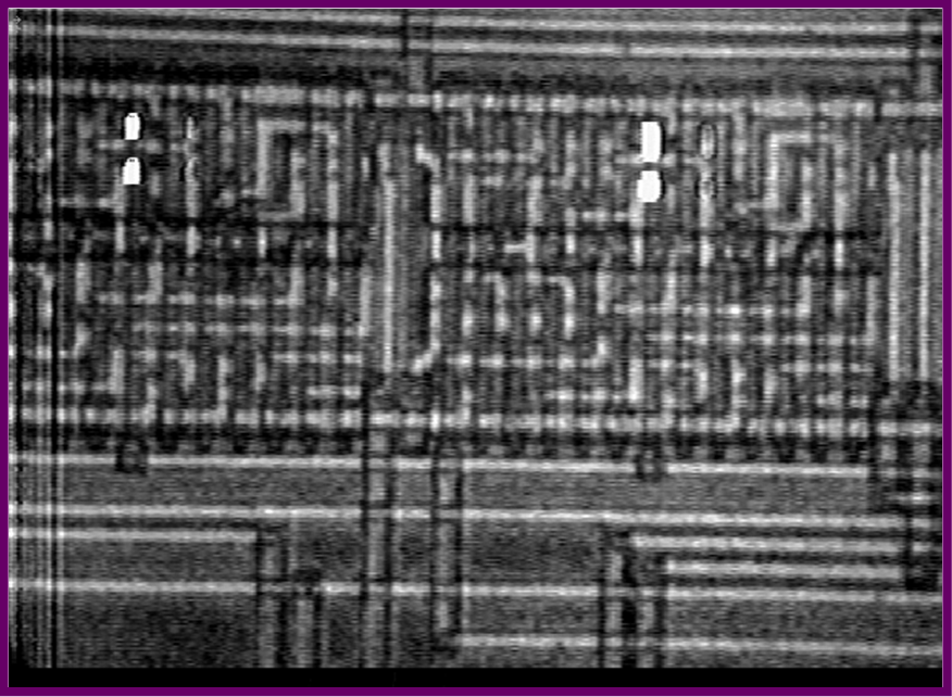
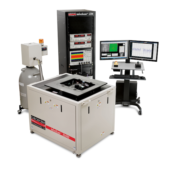
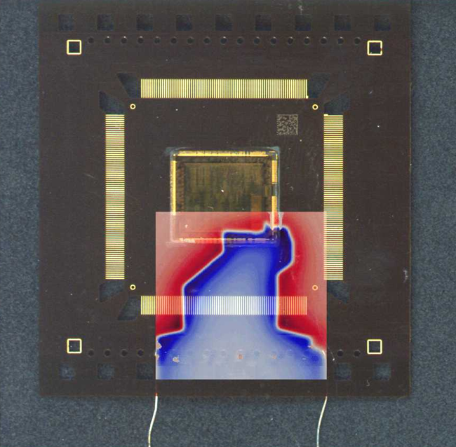
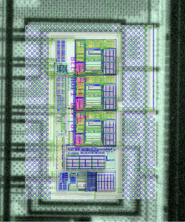
In the past, many problems on semiconductor components could be located and diagnosed using an optical microscope, or a scanning electron microscope. Today's complex integrated circuits can be much more difficult to analyze. This requires a number of defect localization techniques. These techniques include: electron beam techniques, optical beam techniques, photon emission microscopy or light emission, scanned probe techniques, and thermal detection techniques. In addition, one must be able to expose and connect to the area of interest. Chemical unlayering techniques continue to be important; however, a newer tool is rapidly gaining use in this arena - the focused ion beam system.

Estimated Course Duration: 8

Estimated Course Duration: 8
Estimated Course Duration: 8
Estimated Course Duration: 8
Estimated Course Duration: 8
Estimated Course Duration: 8
Estimated Course Duration: 8
Estimated Course Duration: 8
Estimated Course Duration: 8
Estimated Course Duration: 8