If you wish to take a course to receive a certificate, you must take the course under "Online Courses". Do NOT take the course here under "Materials By Topic" as you would not receive a certificate for completing the materials here. The "Materials By Topic" content is intended just for reference purposes.
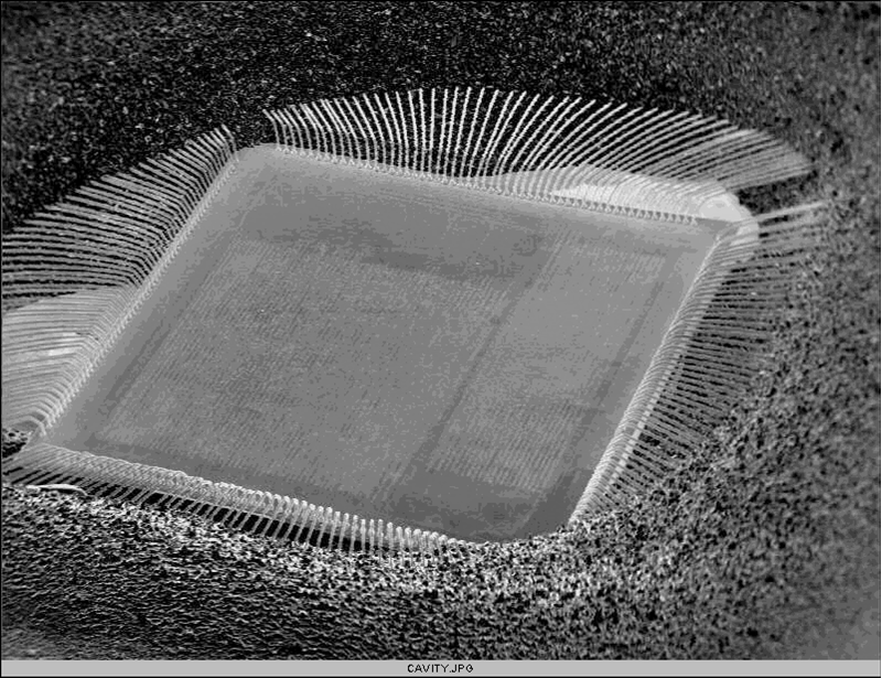
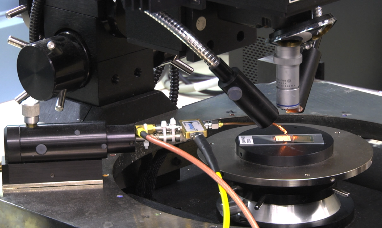
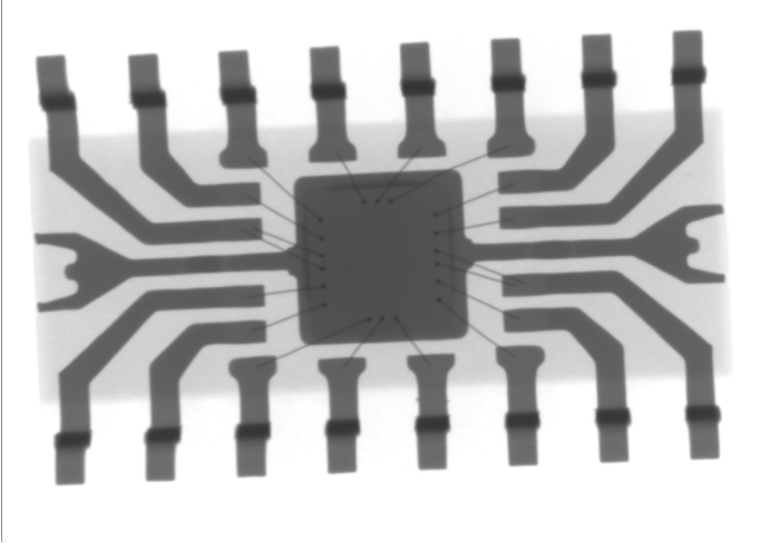
As semiconductor packaging becomes more complex, more analysis is required at the package level. There are several techniques that are used frequently for package level analysis. These include: acoustic microscopy, hermetic seal techniques, optical microscopy, particle impact noise detection (or PIND), and x-ray radiography. In addition to these non-destructive techniques, it is also necessary to have techniques to access or expose the die for further analysis. This access may be from the front side or the back side depending on the device and the information required.
Estimated Course Duration: 8

Estimated Course Duration: 8
Estimated Course Duration: 8
Estimated Course Duration: 8
Estimated Course Duration: 8
Estimated Course Duration: 8
Estimated Course Duration: 8