Materials characterization is an important discipline within the semiconductor manufacturing field. One must be able to identify and characterize topography, vertical structures, aspect ratios, concentrations, dopant distributions, as well as defective conditions and foreign material. Materials characterization can loosely be divided into two groups: imaging techniques and materials analysis techniques.
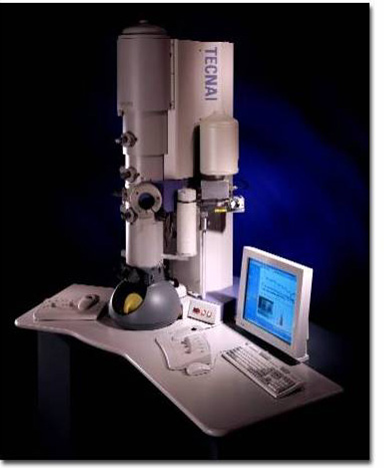
Materials Characterization is occasionally used in failure analysis, and extensively used in yield analysis activities. There are a wide variety of techniques that allow examination of the device surface, as well as the top few microns of a sample. These include techniques like Auger Electron Spectroscopy, which is used for surface analysis, energy dispersive x-ray spectroscopy, which is used for analysis of the top 1 to 5 microns of a sample, Secondary Ion Mass Spectroscopy can be used for both surface analysis and depth profiling, and Transmission Electron Microscopy is used for high resolution imaging of prepared samples.