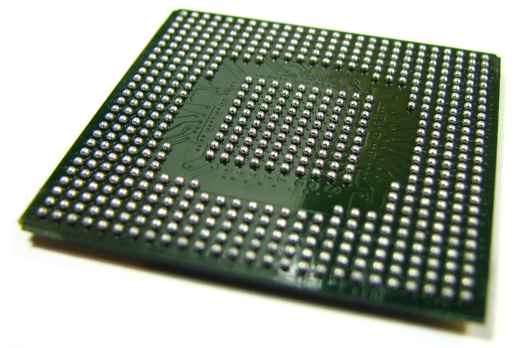
Semiconductor Packaging is increasingly important to the success of almost all electronic systems. Engineers continue to develop and implement packaging approaches and methods that lead to higher performance products, products that take us less physical space, and products that can dissipate increasing amounts of heat. One major area of activity in the past was Flip Chip packaging. Probably the best known flip chip package format is the Ball Grid Array (BGA). Although Flip Chip Packaging is an established technology, there are still areas of development, such as Copper Pillar Technology that is used with this type of packaging. Flip Chip Packages is a 4-hour online course that offers detailed instruction on the technologies used to create Flip Chp Packages. This includes Underfills, Solder Joint Technology and Copper Pillar Technology. We address substrate technology in a separate course, as substrates are used in a variety of different package formats beyond Flip Chip Packages. We place special emphasis on current issues related to manufacturing the current generation products, as well as reliability issues. This course is a must for every manager, engineer and technician working in the semiconductor industry, using semiconductor components or supplying tools to the industry.