Although most people think of Printed Circuit Boards (PCBs) in conjunction with system level design and development, they are actually used quite often in semiconductor product engineering. Many semiconductor firms will design load boards to conduct stress testing and perform production testing, evaluation boards to perform validation work, and application boards to study customer use conditions. Since this is an important topic for Product, Test, and Validation Engineers, we need engineers that are competent in PCB design. This has created a number of challenges related to the packaging of these components. Printed Circuit Board (PCB) Design is a online course that offers detailed instruction on the design printed circuits boards for semiconductor use. We place special emphasis on the overall process. This course is a must for every manager, engineer, and technician working in product, test or validation engineering, or supplying tools to the industry.
By focusing on the fundamentals of PCB design and modeling, participants will learn how to design and specify components for a project. Our instructors work hard to explain PCB design without delving heavily into the complex electrical engineering, and materials science that normally accompany this discipline.
Participants learn basic but powerful aspects about the PCB Design. This skill-building series is divided into four segments:
- PCB Schematic Capture. Participants learn the fundamentals of schematic capture for a printed circuit board design.
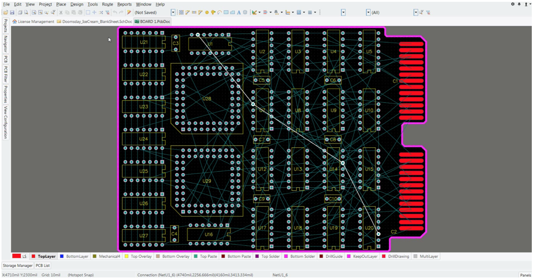
- PCB Place and Route. Participants learn the fundamentals of component placement, and routing of the connections between the components.
- Bill Of Materials. Participants learn about the Bill Of Materials, that is part of the documentation generated for a component PCB design.
- Component Libraries. Participants learn about the component libraries used for generating a populated printed circuit board design.
- The course will provide participants with an overview of the schematic capture and board layout process.
- Participants will understand the basic concepts behind a Bill Of Materials (BOM) for a PCB.
- The course will identify the key issues related to the proper documentation and use of library components.
- The course offers a wide variety of video clips showing the major steps involved in the design and layout process.
- Participants will be able to identify potential problems associated with the design flow.
- Participants will understand how design rules work in conjunction with a board layout.
- Participants will be able to generate the PCB documentation needed to manufacture a PCB.
- Participants will best practices for PCB design.