Electrostatic discharge is a 4 Billion (USD) a year problem for the Semiconductor Industry. This problem is likely to grow in the future as smaller devices are susceptible to damage at lower static voltages and latchup under more subtle conditions. Today, circuit designers and process integration engineers require a fundamental knowledge of device physics and electrothermal behavior of I/O structures in order to develop a process that is robust and can withstand the challenges of today’s varied environments in which ICs are fielded. Layout, ESD pulse behavior, semiconductor physics, and device modeling are all required to produce a successful product. Your industry needs competent engineers and scientists to help achieve these goals. ESD Design and Technology is a 16-hour long course that offers detailed instruction on a variety of subjects pertaining to ESD design and technology. This course is designed for every manager, engineer, and technician concerned with ESD at the I/O design level, the chip level, or supplying ESD tools and simulators to the industry.
Participants learn to develop the skills to determine what constitutes a good ESD design, how to recognize devices that can reduce ESD susceptibility, and how to design new ESD structures for a variety of technologies.
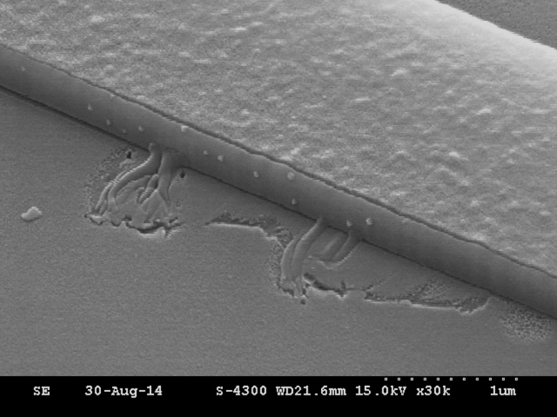
- Overview of the ESD Failure Mechanism. Participants learn the fundamentals of ESD, the physics behind overstress conditions, test equipment, test protocols, and the results of failure.
- ESD Technology Issues. Participants learn the behavior of different IC technologies under various ESD stress conditions. This includes CMOS, bipolar, BiCMOS, SOI GaAs, SiGe, SiGe:C and other strained silicon technologies. Participants also study the response of an IC’s substrates, wells, junctions, dielectric layers, and metallization to ESD.
- ESD Circuit Design Issues. Participants learn how designers develop circuits to protect against ESD damage. This includes MOSFETs, diodes, off-chip driver circuits, receiver circuits, and power clamps.
- Test Strategies. Participants learn the basics on how to test test structures, design screening tests, and how to perform burn-in testing effectively.
- The course will provide participants with an in-depth understanding of the ESD failure mechanism, test structures, equipment, and testing methods used to achieve robust ESD resistance in today’s components.
- Participants will be able to gather ESD data, determine how best to plot the data, and make inferences from that data.
- The course will identify the major issues associated with ESD, explain how they occur, how they are modeled, and how they are mitigated.
- The course can be offered with several textbooks that cover the topic of ESD in much greater detail. The course author is a recognized expert in the field and has written the definitive textbook series on ESD.
- Participants will be able to identify basic ESD structures and how they are used to help reduce ESD susceptibility on semiconductor devices.
- Participants will be able to knowledgeably design ESD structures that are appropriate to assure the robustness of a component.
- Participants will be able to identify appropriate tools to purchase when starting or expanding ESD test capabilities.