Metallography is a basic skill that all electronic failure analysts require. The ability to prepare and analyze a sample material is key to understanding a variety of failure mechanisms, including solder joint failure, package fracturing, board-level and package-level delamination, intermetallic formation, etc. Failed devices, boards and low yields can lead to customer returns and idle manufacturing lines that can cost your company millions of dollars a day. Your industry needs competent analysts to help solve these problems. Metallography is an online course that offers detailed instruction on the techniques required for specimen preparation and analysis. This course is designed for every engineer, and technician working in the electronics field, using electronic components or supplying tools to the industry.
By focusing on a ‘hands-on’ approach to the analysis, participants will learn the appropriate methodology to successfully prepare samples, characterize them, and determine the root cause of failure.
Participants learn to develop the skills to determine what tools and techniques should be applied, and when they should be applied. This skill-building series is divided into two segments:
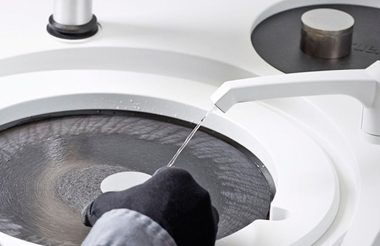
- Sample Preparation. Participants learn about the techniques for preparing material sample for analysis. This includes choosing the proper sample orientation, cross-sections, decorations (etching the surface of the material), and when to use sample coatings.
- Imaging Techniques. Participants learn how to use both the optical and scanning electron microscope to image samples. They also learn how to use the tools to identify items like grain structure, alloying, thermal damage, corrosion, etc.
- The course will provide participants with an in-depth understanding of how to prepare a sample for imaging.
- Participants will be able to perform cross-sections on a variety of different materials.
- Participants will be able to determine the best approach to sectioning a sample, based on the material type.
- Participants will be able to identify basic material features on electronic components and boards.
- Participants will be able to properly use the optical and scanning electron microscopes for imaging samples.
- Participants will be able to identify the appropriate etch to highlight features on a sample.